


Key Insights
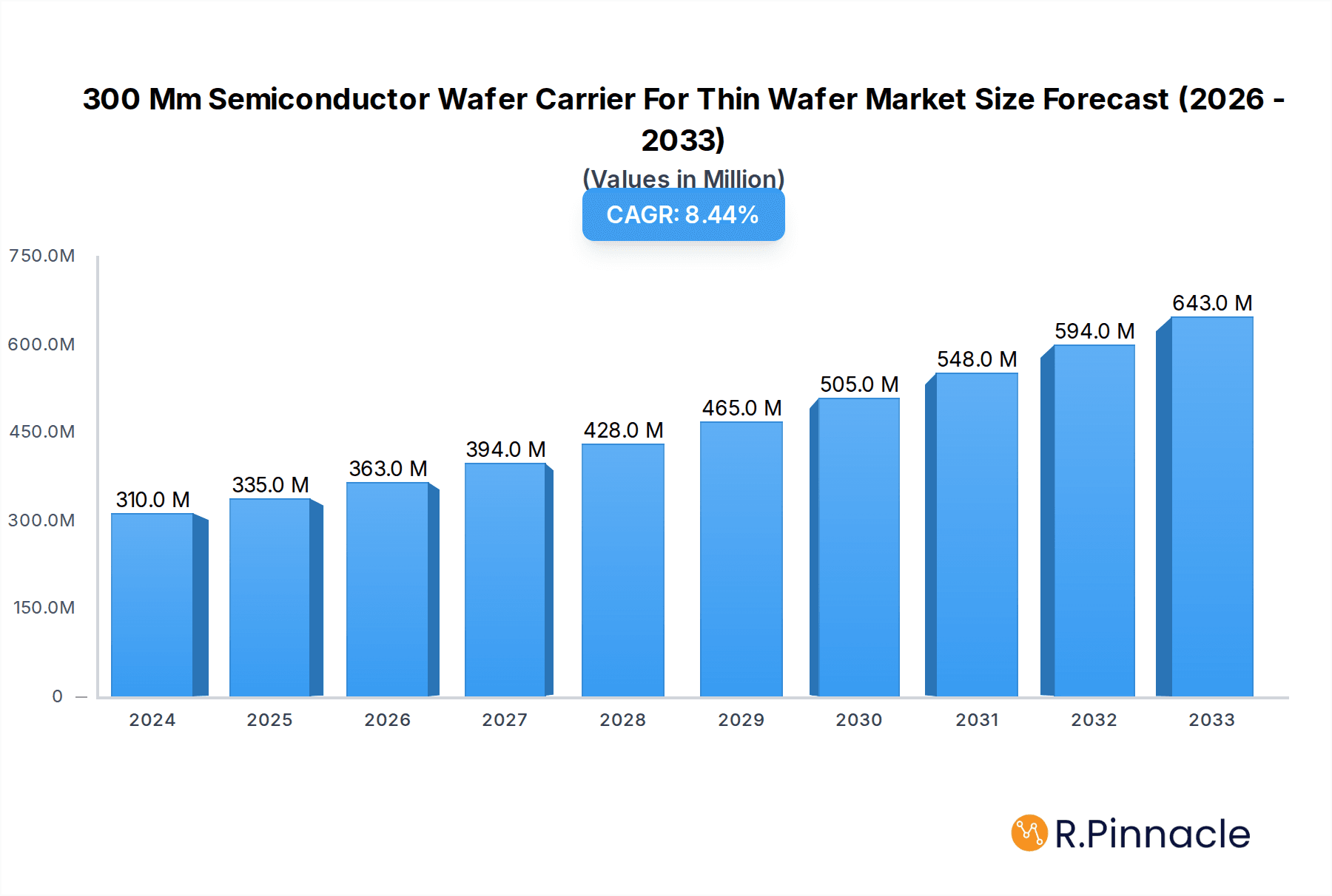
The global market for 300mm semiconductor wafer carriers, specifically designed for thin wafers, is poised for significant expansion, with an estimated market size of $335 million in 2025. This sector is projected to witness robust growth, driven by a compound annual growth rate (CAGR) of 8.2% from 2019 to 2033. A primary catalyst for this growth is the increasing demand for advanced semiconductor devices that require thinner wafers for enhanced performance and miniaturization. The continuous technological advancements in the semiconductor industry, coupled with the escalating adoption of cutting-edge technologies like Artificial Intelligence (AI), 5G, and the Internet of Things (IoT), are fueling the need for more sophisticated and efficient wafer handling solutions. Key applications within this market include Integrated Device Manufacturers (IDMs) and Foundries, underscoring the broad adoption across the semiconductor manufacturing ecosystem.

300 Mm Semiconductor Wafer Carrier For Thin Wafer Market Size (In Million)

Further analysis reveals that the market will be significantly shaped by the prevailing trends in wafer processing and handling. The increasing prevalence of thin wafer technologies, essential for next-generation mobile devices, advanced packaging, and high-performance computing, necessitates specialized carriers that offer superior protection and precision during manufacturing and transportation. While the market is characterized by strong growth drivers, potential restraints such as the high cost of advanced manufacturing equipment and the stringent quality control requirements could pose challenges. However, the innovative product developments from leading companies like Entegris and Shin-Etsu Polymer, alongside the strategic expansion of production capacities by players such as Miraial and 3S Korea, are expected to mitigate these challenges and sustain the upward trajectory. The market's segmentation by type, including FOUP (Front-Opening Unified Pod) and FOSB (Front Opening Shipping Box), reflects the diverse needs of the semiconductor supply chain, with a focus on ensuring wafer integrity throughout the entire process.
300 Mm Semiconductor Wafer Carrier For Thin Wafer Company Market Share
300 Mm Semiconductor Wafer Carrier For Thin Wafer Market Insights: A Comprehensive Analysis (2019-2033)
This in-depth market report provides a granular analysis of the 300 mm semiconductor wafer carrier for thin wafer market, crucial for safeguarding and transporting ultra-thin silicon wafers in advanced semiconductor manufacturing. The study covers the historical period of 2019–2024, with a base year of 2025 and a forecast period extending to 2033. It delves into market structure, dynamics, regional dominance, product innovations, and the strategic moves of key industry players. Understand the evolving landscape driven by the increasing demand for high-performance semiconductor devices, miniaturization, and the adoption of advanced packaging technologies. This report is essential for IDM (Integrated Device Manufacturer) and Foundry segments, offering actionable insights for stakeholders involved with FOUP (Front Opening Unified Pod) and FOSB (Front Opening Shipping Box) technologies.
300 Mm Semiconductor Wafer Carrier For Thin Wafer Market Structure & Innovation Trends
The 300 mm semiconductor wafer carrier for thin wafer market exhibits a moderate to high level of market concentration, with a few dominant players holding significant market share. Key innovators are continuously developing advanced carrier designs to accommodate the ever-decreasing thickness of semiconductor wafers, driven by the need for improved chip performance and reduced form factors. Regulatory frameworks, primarily focused on material purity, electrostatic discharge (ESD) protection, and cleanroom compatibility, play a vital role in shaping product development. The threat of product substitutes is relatively low due to the specialized nature of these carriers, but advancements in alternative wafer handling methods could emerge. End-user demographics are predominantly large-scale semiconductor manufacturers, including IDMs and Foundries, seeking reliable and contamination-free solutions. Mergers and acquisitions (M&A) activities, with deal values potentially reaching into the hundreds of millions, are observed as companies aim to expand their product portfolios, geographic reach, and technological capabilities. Recent M&A activities have focused on acquiring niche technologies related to advanced materials and miniaturized carrier designs.
300 Mm Semiconductor Wafer Carrier For Thin Wafer Market Dynamics & Trends
The 300 mm semiconductor wafer carrier for thin wafer market is experiencing robust growth, propelled by the insatiable global demand for sophisticated semiconductor devices. The relentless pursuit of miniaturization in consumer electronics, the expansion of 5G infrastructure, and the burgeoning adoption of Artificial Intelligence (AI) and Machine Learning (ML) are significant growth drivers. Technological disruptions, such as the development of novel materials for enhanced wafer protection and reduced particle generation, are reshaping the competitive landscape. Consumer preferences, dictated by the stringent requirements of advanced semiconductor fabrication, favor carriers that offer superior cleanliness, mechanical stability for ultra-thin wafers, and compatibility with automated handling systems. Competitive dynamics are characterized by intense innovation, strategic partnerships, and a focus on delivering cost-effective yet high-performance solutions. The market penetration of specialized thin wafer carriers is steadily increasing as wafer thinning processes become more prevalent across the semiconductor industry. Emerging trends include the integration of smart features for real-time monitoring of wafer conditions and the development of carriers designed for the unique demands of wafer-level packaging. The Compound Annual Growth Rate (CAGR) for this market is projected to be robust, reflecting the ongoing expansion of the semiconductor ecosystem.
Dominant Regions & Segments in 300 Mm Semiconductor Wafer Carrier For Thin Wafer
Asia-Pacific, particularly Taiwan and South Korea, currently dominates the 300 mm semiconductor wafer carrier for thin wafer market. This regional dominance is underpinned by the presence of leading semiconductor foundries and IDMs, significant government investments in the semiconductor industry, and a highly developed manufacturing infrastructure. Economic policies in these regions often favor technological advancement and manufacturing prowess, creating a fertile ground for market growth. The Foundry segment is a key driver of this dominance, with manufacturers increasingly relying on specialized carriers for their advanced node manufacturing processes. Within the FOUP type, advancements in sealing technologies and material science are critical for maintaining wafer integrity.
Leading Region: Asia-Pacific
- Key Countries: Taiwan, South Korea, China
- Drivers: High concentration of wafer fabrication plants, government incentives for semiconductor manufacturing, strong R&D capabilities.
Dominant Segments:
- Application: Foundry: Foundries are at the forefront of demanding specialized wafer carriers due to their role in producing advanced chips for various end-use applications. The need to handle increasingly thin wafers from 0.075 millimeters to 0.1 millimeters in thickness for cutting-edge technologies like high-performance computing and AI processors makes specialized carriers indispensable.
- Type: FOUP: Front Opening Unified Pods (FOUPs) are the preferred choice for in-fab wafer transport and storage. Innovations in FOUP design focus on minimizing particle generation, enhancing ESD protection, and ensuring robust mechanical support for delicate, thin wafers. The market for FOUPs in this segment is projected to grow significantly due to their widespread adoption in state-of-the-art fabrication facilities.
300 Mm Semiconductor Wafer Carrier For Thin Wafer Product Innovations
Product innovations in the 300 mm semiconductor wafer carrier for thin wafer market are centered around materials science and advanced design. Manufacturers are developing carriers from ultra-clean, high-purity polymers that exhibit superior mechanical strength and dimensional stability, crucial for handling wafer thicknesses as low as 0.075 millimeters. Innovations include enhanced ESD protection features, improved particle reduction technologies, and designs that minimize contact points with the wafer surface to prevent scratching or contamination. These advancements provide a significant competitive advantage by ensuring higher wafer yields and greater reliability in critical manufacturing steps.
Report Scope & Segmentation Analysis
This report segments the 300 mm semiconductor wafer carrier for thin wafer market based on Application into IDM and Foundry, and by Type into FOUP and FOSB.
- Application: IDM: Integrated Device Manufacturers will continue to require advanced carriers for their internal wafer production, focusing on cost-effectiveness and process integration. Growth projections for this segment are steady, driven by ongoing investments in new fabrication facilities.
- Application: Foundry: The Foundry segment is expected to exhibit higher growth rates due to its role in catering to the diverse needs of fabless semiconductor companies and the rapid adoption of new wafer technologies. Market sizes are substantial, with significant opportunities in advanced node manufacturing.
- Type: FOUP: Front Opening Unified Pods represent the largest segment due to their primary use in fab environments. Forecasted growth is robust, driven by the increasing number of wafer starts globally.
- Type: FOSB: Front Opening Shipping Boxes are vital for inter-facility wafer transport. While a smaller segment, it is experiencing steady growth as supply chains become more globalized and interdependencies increase.
Key Drivers of 300 Mm Semiconductor Wafer Carrier For Thin Wafer Growth
The growth of the 300 mm semiconductor wafer carrier for thin wafer market is primarily driven by the escalating demand for advanced semiconductor devices. The increasing complexity and miniaturization of integrated circuits necessitate wafer handling solutions that can accommodate thinner wafers with enhanced precision and protection. Technological advancements in wafer thinning processes, such as grinding and etching, are making thinner wafers more accessible for a wider range of applications, including next-generation mobile devices, high-performance computing, and automotive electronics. Furthermore, the expansion of the semiconductor manufacturing capacity globally, particularly in emerging markets, fuels the demand for these specialized carriers. Government initiatives promoting domestic semiconductor production and innovation also contribute significantly to market expansion.
Challenges in the 300 Mm Semiconductor Wafer Carrier For Thin Wafer Sector
Despite the strong growth prospects, the 300 mm semiconductor wafer carrier for thin wafer sector faces several challenges. The stringent purity requirements of semiconductor manufacturing demand extremely low levels of particle generation and chemical contamination from the carriers, necessitating advanced material science and rigorous quality control. The increasing thinness of wafers also introduces mechanical fragility, posing challenges in designing carriers that provide sufficient support without causing damage or stress. Supply chain disruptions, geopolitical tensions, and the rising cost of high-purity raw materials can impact production costs and availability. Additionally, the rapid pace of technological innovation requires continuous investment in R&D to keep pace with evolving wafer processing techniques and end-product demands.
Emerging Opportunities in 300 Mm Semiconductor Wafer Carrier For Thin Wafer
Emerging opportunities within the 300 mm semiconductor wafer carrier for thin wafer market are abundant, driven by the continuous evolution of the semiconductor industry. The increasing adoption of wafer-level packaging (WLP) and advanced packaging technologies presents new demands for specialized carriers that can handle integrated wafer-level structures. The growing importance of the automotive semiconductor segment, with its increasing demand for high-reliability and advanced chips, opens up new avenues for growth. Furthermore, the development of "smart" carriers equipped with sensors for real-time monitoring of wafer conditions, such as temperature and humidity, offers opportunities for enhanced process control and yield improvement. The expansion of semiconductor manufacturing in new geographic regions also presents significant untapped market potential.
Leading Players in the 300 Mm Semiconductor Wafer Carrier For Thin Wafer Market
- Entegris
- Shin-Etsu Polymer
- Miraial
- 3S Korea
- Chuang King Enterprise
- Dainichi Shoji
- Gudeng Precision
Key Developments in 300 Mm Semiconductor Wafer Carrier For Thin Wafer Industry
- 2023: Launch of new FOUP designs with enhanced particle reduction features for sub-5nm semiconductor manufacturing.
- 2022: Acquisition of a specialized polymer compounding company by a leading carrier manufacturer to secure advanced material supply.
- 2021: Introduction of FOSBs with improved vibration dampening for high-value wafer shipments.
- 2020: Development of novel materials for ultra-thin wafer carriers, offering improved rigidity and reduced outgassing.
- 2019: Increased investment in R&D for carriers supporting advanced lithography processes and next-generation memory technologies.
Future Outlook for 300 Mm Semiconductor Wafer Carrier For Thin Wafer Market
The future outlook for the 300 mm semiconductor wafer carrier for thin wafer market is exceptionally bright, fueled by sustained innovation and the ever-growing global appetite for advanced semiconductor technology. The increasing adoption of AI, the expansion of IoT devices, and the ongoing development of next-generation communication networks will continue to drive demand for higher performance and more compact semiconductor components, necessitating the handling of increasingly thinner wafers. Innovations in carrier materials and design will focus on ultra-high purity, superior mechanical protection, and integration with automation systems. Strategic partnerships and potential M&A activities are expected to shape the competitive landscape, with companies striving to gain a technological edge and expand their market reach. The market is poised for continued expansion, offering significant opportunities for stakeholders who can adapt to the evolving technological requirements and stringent quality standards of the semiconductor industry.
300 Mm Semiconductor Wafer Carrier For Thin Wafer Segmentation
-
1. Application
- 1.1. IDM
- 1.2. Foundry
-
2. Type
- 2.1. FOUP
- 2.2. FOSB
300 Mm Semiconductor Wafer Carrier For Thin Wafer Segmentation By Geography
-
1. North America
- 1.1. United States
- 1.2. Canada
- 1.3. Mexico
-
2. South America
- 2.1. Brazil
- 2.2. Argentina
- 2.3. Rest of South America
-
3. Europe
- 3.1. United Kingdom
- 3.2. Germany
- 3.3. France
- 3.4. Italy
- 3.5. Spain
- 3.6. Russia
- 3.7. Benelux
- 3.8. Nordics
- 3.9. Rest of Europe
-
4. Middle East & Africa
- 4.1. Turkey
- 4.2. Israel
- 4.3. GCC
- 4.4. North Africa
- 4.5. South Africa
- 4.6. Rest of Middle East & Africa
-
5. Asia Pacific
- 5.1. China
- 5.2. India
- 5.3. Japan
- 5.4. South Korea
- 5.5. ASEAN
- 5.6. Oceania
- 5.7. Rest of Asia Pacific
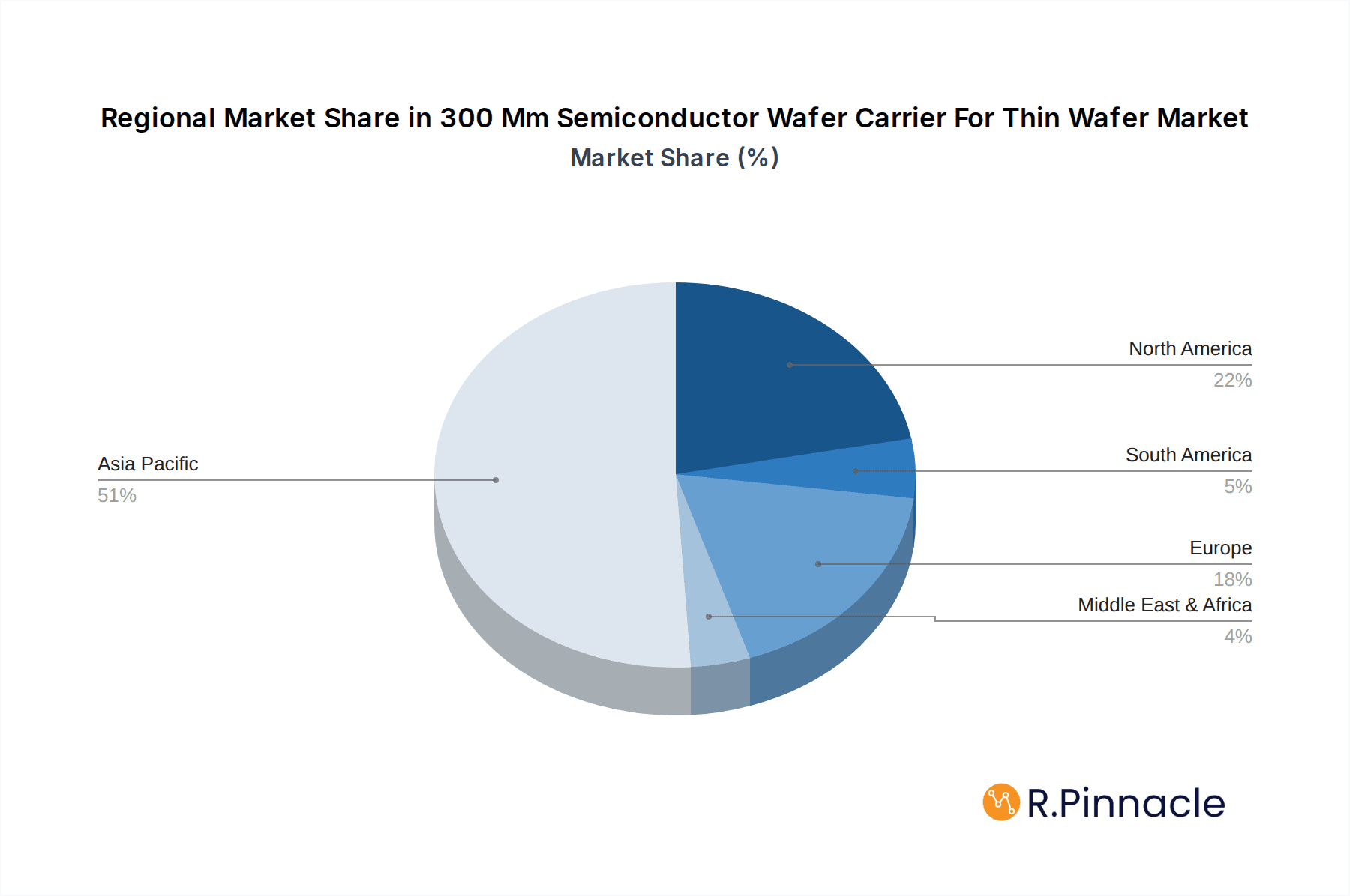
300 Mm Semiconductor Wafer Carrier For Thin Wafer Regional Market Share
Geographic Coverage of 300 Mm Semiconductor Wafer Carrier For Thin Wafer
300 Mm Semiconductor Wafer Carrier For Thin Wafer REPORT HIGHLIGHTS
| Aspects | Details |
|---|---|
| Study Period | 2020-2034 |
| Base Year | 2025 |
| Estimated Year | 2026 |
| Forecast Period | 2026-2034 |
| Historical Period | 2020-2025 |
| Growth Rate | CAGR of 8.2% from 2020-2034 |
| Segmentation |
|
Table of Contents
- 1. Introduction
- 1.1. Research Scope
- 1.2. Market Segmentation
- 1.3. Research Methodology
- 1.4. Definitions and Assumptions
- 2. Executive Summary
- 2.1. Introduction
- 3. Market Dynamics
- 3.1. Introduction
- 3.2. Market Drivers
- 3.3. Market Restrains
- 3.4. Market Trends
- 4. Market Factor Analysis
- 4.1. Porters Five Forces
- 4.2. Supply/Value Chain
- 4.3. PESTEL analysis
- 4.4. Market Entropy
- 4.5. Patent/Trademark Analysis
- 5. Global 300 Mm Semiconductor Wafer Carrier For Thin Wafer Analysis, Insights and Forecast, 2020-2032
- 5.1. Market Analysis, Insights and Forecast - by Application
- 5.1.1. IDM
- 5.1.2. Foundry
- 5.2. Market Analysis, Insights and Forecast - by Type
- 5.2.1. FOUP
- 5.2.2. FOSB
- 5.3. Market Analysis, Insights and Forecast - by Region
- 5.3.1. North America
- 5.3.2. South America
- 5.3.3. Europe
- 5.3.4. Middle East & Africa
- 5.3.5. Asia Pacific
- 5.1. Market Analysis, Insights and Forecast - by Application
- 6. North America 300 Mm Semiconductor Wafer Carrier For Thin Wafer Analysis, Insights and Forecast, 2020-2032
- 6.1. Market Analysis, Insights and Forecast - by Application
- 6.1.1. IDM
- 6.1.2. Foundry
- 6.2. Market Analysis, Insights and Forecast - by Type
- 6.2.1. FOUP
- 6.2.2. FOSB
- 6.1. Market Analysis, Insights and Forecast - by Application
- 7. South America 300 Mm Semiconductor Wafer Carrier For Thin Wafer Analysis, Insights and Forecast, 2020-2032
- 7.1. Market Analysis, Insights and Forecast - by Application
- 7.1.1. IDM
- 7.1.2. Foundry
- 7.2. Market Analysis, Insights and Forecast - by Type
- 7.2.1. FOUP
- 7.2.2. FOSB
- 7.1. Market Analysis, Insights and Forecast - by Application
- 8. Europe 300 Mm Semiconductor Wafer Carrier For Thin Wafer Analysis, Insights and Forecast, 2020-2032
- 8.1. Market Analysis, Insights and Forecast - by Application
- 8.1.1. IDM
- 8.1.2. Foundry
- 8.2. Market Analysis, Insights and Forecast - by Type
- 8.2.1. FOUP
- 8.2.2. FOSB
- 8.1. Market Analysis, Insights and Forecast - by Application
- 9. Middle East & Africa 300 Mm Semiconductor Wafer Carrier For Thin Wafer Analysis, Insights and Forecast, 2020-2032
- 9.1. Market Analysis, Insights and Forecast - by Application
- 9.1.1. IDM
- 9.1.2. Foundry
- 9.2. Market Analysis, Insights and Forecast - by Type
- 9.2.1. FOUP
- 9.2.2. FOSB
- 9.1. Market Analysis, Insights and Forecast - by Application
- 10. Asia Pacific 300 Mm Semiconductor Wafer Carrier For Thin Wafer Analysis, Insights and Forecast, 2020-2032
- 10.1. Market Analysis, Insights and Forecast - by Application
- 10.1.1. IDM
- 10.1.2. Foundry
- 10.2. Market Analysis, Insights and Forecast - by Type
- 10.2.1. FOUP
- 10.2.2. FOSB
- 10.1. Market Analysis, Insights and Forecast - by Application
- 11. Competitive Analysis
- 11.1. Global Market Share Analysis 2025
- 11.2. Company Profiles
- 11.2.1 Entegris
- 11.2.1.1. Overview
- 11.2.1.2. Products
- 11.2.1.3. SWOT Analysis
- 11.2.1.4. Recent Developments
- 11.2.1.5. Financials (Based on Availability)
- 11.2.2 Shin-Etsu Polymer
- 11.2.2.1. Overview
- 11.2.2.2. Products
- 11.2.2.3. SWOT Analysis
- 11.2.2.4. Recent Developments
- 11.2.2.5. Financials (Based on Availability)
- 11.2.3 Miraial
- 11.2.3.1. Overview
- 11.2.3.2. Products
- 11.2.3.3. SWOT Analysis
- 11.2.3.4. Recent Developments
- 11.2.3.5. Financials (Based on Availability)
- 11.2.4 3S Korea
- 11.2.4.1. Overview
- 11.2.4.2. Products
- 11.2.4.3. SWOT Analysis
- 11.2.4.4. Recent Developments
- 11.2.4.5. Financials (Based on Availability)
- 11.2.5 Chuang King Enterprise
- 11.2.5.1. Overview
- 11.2.5.2. Products
- 11.2.5.3. SWOT Analysis
- 11.2.5.4. Recent Developments
- 11.2.5.5. Financials (Based on Availability)
- 11.2.6 Dainichi Shoji
- 11.2.6.1. Overview
- 11.2.6.2. Products
- 11.2.6.3. SWOT Analysis
- 11.2.6.4. Recent Developments
- 11.2.6.5. Financials (Based on Availability)
- 11.2.7 Gudeng Precision
- 11.2.7.1. Overview
- 11.2.7.2. Products
- 11.2.7.3. SWOT Analysis
- 11.2.7.4. Recent Developments
- 11.2.7.5. Financials (Based on Availability)
- 11.2.1 Entegris
List of Figures
- Figure 1: Global 300 Mm Semiconductor Wafer Carrier For Thin Wafer Revenue Breakdown (million, %) by Region 2025 & 2033
- Figure 2: North America 300 Mm Semiconductor Wafer Carrier For Thin Wafer Revenue (million), by Application 2025 & 2033
- Figure 3: North America 300 Mm Semiconductor Wafer Carrier For Thin Wafer Revenue Share (%), by Application 2025 & 2033
- Figure 4: North America 300 Mm Semiconductor Wafer Carrier For Thin Wafer Revenue (million), by Type 2025 & 2033
- Figure 5: North America 300 Mm Semiconductor Wafer Carrier For Thin Wafer Revenue Share (%), by Type 2025 & 2033
- Figure 6: North America 300 Mm Semiconductor Wafer Carrier For Thin Wafer Revenue (million), by Country 2025 & 2033
- Figure 7: North America 300 Mm Semiconductor Wafer Carrier For Thin Wafer Revenue Share (%), by Country 2025 & 2033
- Figure 8: South America 300 Mm Semiconductor Wafer Carrier For Thin Wafer Revenue (million), by Application 2025 & 2033
- Figure 9: South America 300 Mm Semiconductor Wafer Carrier For Thin Wafer Revenue Share (%), by Application 2025 & 2033
- Figure 10: South America 300 Mm Semiconductor Wafer Carrier For Thin Wafer Revenue (million), by Type 2025 & 2033
- Figure 11: South America 300 Mm Semiconductor Wafer Carrier For Thin Wafer Revenue Share (%), by Type 2025 & 2033
- Figure 12: South America 300 Mm Semiconductor Wafer Carrier For Thin Wafer Revenue (million), by Country 2025 & 2033
- Figure 13: South America 300 Mm Semiconductor Wafer Carrier For Thin Wafer Revenue Share (%), by Country 2025 & 2033
- Figure 14: Europe 300 Mm Semiconductor Wafer Carrier For Thin Wafer Revenue (million), by Application 2025 & 2033
- Figure 15: Europe 300 Mm Semiconductor Wafer Carrier For Thin Wafer Revenue Share (%), by Application 2025 & 2033
- Figure 16: Europe 300 Mm Semiconductor Wafer Carrier For Thin Wafer Revenue (million), by Type 2025 & 2033
- Figure 17: Europe 300 Mm Semiconductor Wafer Carrier For Thin Wafer Revenue Share (%), by Type 2025 & 2033
- Figure 18: Europe 300 Mm Semiconductor Wafer Carrier For Thin Wafer Revenue (million), by Country 2025 & 2033
- Figure 19: Europe 300 Mm Semiconductor Wafer Carrier For Thin Wafer Revenue Share (%), by Country 2025 & 2033
- Figure 20: Middle East & Africa 300 Mm Semiconductor Wafer Carrier For Thin Wafer Revenue (million), by Application 2025 & 2033
- Figure 21: Middle East & Africa 300 Mm Semiconductor Wafer Carrier For Thin Wafer Revenue Share (%), by Application 2025 & 2033
- Figure 22: Middle East & Africa 300 Mm Semiconductor Wafer Carrier For Thin Wafer Revenue (million), by Type 2025 & 2033
- Figure 23: Middle East & Africa 300 Mm Semiconductor Wafer Carrier For Thin Wafer Revenue Share (%), by Type 2025 & 2033
- Figure 24: Middle East & Africa 300 Mm Semiconductor Wafer Carrier For Thin Wafer Revenue (million), by Country 2025 & 2033
- Figure 25: Middle East & Africa 300 Mm Semiconductor Wafer Carrier For Thin Wafer Revenue Share (%), by Country 2025 & 2033
- Figure 26: Asia Pacific 300 Mm Semiconductor Wafer Carrier For Thin Wafer Revenue (million), by Application 2025 & 2033
- Figure 27: Asia Pacific 300 Mm Semiconductor Wafer Carrier For Thin Wafer Revenue Share (%), by Application 2025 & 2033
- Figure 28: Asia Pacific 300 Mm Semiconductor Wafer Carrier For Thin Wafer Revenue (million), by Type 2025 & 2033
- Figure 29: Asia Pacific 300 Mm Semiconductor Wafer Carrier For Thin Wafer Revenue Share (%), by Type 2025 & 2033
- Figure 30: Asia Pacific 300 Mm Semiconductor Wafer Carrier For Thin Wafer Revenue (million), by Country 2025 & 2033
- Figure 31: Asia Pacific 300 Mm Semiconductor Wafer Carrier For Thin Wafer Revenue Share (%), by Country 2025 & 2033
List of Tables
- Table 1: Global 300 Mm Semiconductor Wafer Carrier For Thin Wafer Revenue million Forecast, by Application 2020 & 2033
- Table 2: Global 300 Mm Semiconductor Wafer Carrier For Thin Wafer Revenue million Forecast, by Type 2020 & 2033
- Table 3: Global 300 Mm Semiconductor Wafer Carrier For Thin Wafer Revenue million Forecast, by Region 2020 & 2033
- Table 4: Global 300 Mm Semiconductor Wafer Carrier For Thin Wafer Revenue million Forecast, by Application 2020 & 2033
- Table 5: Global 300 Mm Semiconductor Wafer Carrier For Thin Wafer Revenue million Forecast, by Type 2020 & 2033
- Table 6: Global 300 Mm Semiconductor Wafer Carrier For Thin Wafer Revenue million Forecast, by Country 2020 & 2033
- Table 7: United States 300 Mm Semiconductor Wafer Carrier For Thin Wafer Revenue (million) Forecast, by Application 2020 & 2033
- Table 8: Canada 300 Mm Semiconductor Wafer Carrier For Thin Wafer Revenue (million) Forecast, by Application 2020 & 2033
- Table 9: Mexico 300 Mm Semiconductor Wafer Carrier For Thin Wafer Revenue (million) Forecast, by Application 2020 & 2033
- Table 10: Global 300 Mm Semiconductor Wafer Carrier For Thin Wafer Revenue million Forecast, by Application 2020 & 2033
- Table 11: Global 300 Mm Semiconductor Wafer Carrier For Thin Wafer Revenue million Forecast, by Type 2020 & 2033
- Table 12: Global 300 Mm Semiconductor Wafer Carrier For Thin Wafer Revenue million Forecast, by Country 2020 & 2033
- Table 13: Brazil 300 Mm Semiconductor Wafer Carrier For Thin Wafer Revenue (million) Forecast, by Application 2020 & 2033
- Table 14: Argentina 300 Mm Semiconductor Wafer Carrier For Thin Wafer Revenue (million) Forecast, by Application 2020 & 2033
- Table 15: Rest of South America 300 Mm Semiconductor Wafer Carrier For Thin Wafer Revenue (million) Forecast, by Application 2020 & 2033
- Table 16: Global 300 Mm Semiconductor Wafer Carrier For Thin Wafer Revenue million Forecast, by Application 2020 & 2033
- Table 17: Global 300 Mm Semiconductor Wafer Carrier For Thin Wafer Revenue million Forecast, by Type 2020 & 2033
- Table 18: Global 300 Mm Semiconductor Wafer Carrier For Thin Wafer Revenue million Forecast, by Country 2020 & 2033
- Table 19: United Kingdom 300 Mm Semiconductor Wafer Carrier For Thin Wafer Revenue (million) Forecast, by Application 2020 & 2033
- Table 20: Germany 300 Mm Semiconductor Wafer Carrier For Thin Wafer Revenue (million) Forecast, by Application 2020 & 2033
- Table 21: France 300 Mm Semiconductor Wafer Carrier For Thin Wafer Revenue (million) Forecast, by Application 2020 & 2033
- Table 22: Italy 300 Mm Semiconductor Wafer Carrier For Thin Wafer Revenue (million) Forecast, by Application 2020 & 2033
- Table 23: Spain 300 Mm Semiconductor Wafer Carrier For Thin Wafer Revenue (million) Forecast, by Application 2020 & 2033
- Table 24: Russia 300 Mm Semiconductor Wafer Carrier For Thin Wafer Revenue (million) Forecast, by Application 2020 & 2033
- Table 25: Benelux 300 Mm Semiconductor Wafer Carrier For Thin Wafer Revenue (million) Forecast, by Application 2020 & 2033
- Table 26: Nordics 300 Mm Semiconductor Wafer Carrier For Thin Wafer Revenue (million) Forecast, by Application 2020 & 2033
- Table 27: Rest of Europe 300 Mm Semiconductor Wafer Carrier For Thin Wafer Revenue (million) Forecast, by Application 2020 & 2033
- Table 28: Global 300 Mm Semiconductor Wafer Carrier For Thin Wafer Revenue million Forecast, by Application 2020 & 2033
- Table 29: Global 300 Mm Semiconductor Wafer Carrier For Thin Wafer Revenue million Forecast, by Type 2020 & 2033
- Table 30: Global 300 Mm Semiconductor Wafer Carrier For Thin Wafer Revenue million Forecast, by Country 2020 & 2033
- Table 31: Turkey 300 Mm Semiconductor Wafer Carrier For Thin Wafer Revenue (million) Forecast, by Application 2020 & 2033
- Table 32: Israel 300 Mm Semiconductor Wafer Carrier For Thin Wafer Revenue (million) Forecast, by Application 2020 & 2033
- Table 33: GCC 300 Mm Semiconductor Wafer Carrier For Thin Wafer Revenue (million) Forecast, by Application 2020 & 2033
- Table 34: North Africa 300 Mm Semiconductor Wafer Carrier For Thin Wafer Revenue (million) Forecast, by Application 2020 & 2033
- Table 35: South Africa 300 Mm Semiconductor Wafer Carrier For Thin Wafer Revenue (million) Forecast, by Application 2020 & 2033
- Table 36: Rest of Middle East & Africa 300 Mm Semiconductor Wafer Carrier For Thin Wafer Revenue (million) Forecast, by Application 2020 & 2033
- Table 37: Global 300 Mm Semiconductor Wafer Carrier For Thin Wafer Revenue million Forecast, by Application 2020 & 2033
- Table 38: Global 300 Mm Semiconductor Wafer Carrier For Thin Wafer Revenue million Forecast, by Type 2020 & 2033
- Table 39: Global 300 Mm Semiconductor Wafer Carrier For Thin Wafer Revenue million Forecast, by Country 2020 & 2033
- Table 40: China 300 Mm Semiconductor Wafer Carrier For Thin Wafer Revenue (million) Forecast, by Application 2020 & 2033
- Table 41: India 300 Mm Semiconductor Wafer Carrier For Thin Wafer Revenue (million) Forecast, by Application 2020 & 2033
- Table 42: Japan 300 Mm Semiconductor Wafer Carrier For Thin Wafer Revenue (million) Forecast, by Application 2020 & 2033
- Table 43: South Korea 300 Mm Semiconductor Wafer Carrier For Thin Wafer Revenue (million) Forecast, by Application 2020 & 2033
- Table 44: ASEAN 300 Mm Semiconductor Wafer Carrier For Thin Wafer Revenue (million) Forecast, by Application 2020 & 2033
- Table 45: Oceania 300 Mm Semiconductor Wafer Carrier For Thin Wafer Revenue (million) Forecast, by Application 2020 & 2033
- Table 46: Rest of Asia Pacific 300 Mm Semiconductor Wafer Carrier For Thin Wafer Revenue (million) Forecast, by Application 2020 & 2033
Frequently Asked Questions
1. What is the projected Compound Annual Growth Rate (CAGR) of the 300 Mm Semiconductor Wafer Carrier For Thin Wafer?
The projected CAGR is approximately 8.2%.
2. Which companies are prominent players in the 300 Mm Semiconductor Wafer Carrier For Thin Wafer?
Key companies in the market include Entegris, Shin-Etsu Polymer, Miraial, 3S Korea, Chuang King Enterprise, Dainichi Shoji, Gudeng Precision.
3. What are the main segments of the 300 Mm Semiconductor Wafer Carrier For Thin Wafer?
The market segments include Application, Type.
4. Can you provide details about the market size?
The market size is estimated to be USD 335 million as of 2022.
5. What are some drivers contributing to market growth?
N/A
6. What are the notable trends driving market growth?
N/A
7. Are there any restraints impacting market growth?
N/A
8. Can you provide examples of recent developments in the market?
N/A
9. What pricing options are available for accessing the report?
Pricing options include single-user, multi-user, and enterprise licenses priced at USD 2900.00, USD 4350.00, and USD 5800.00 respectively.
10. Is the market size provided in terms of value or volume?
The market size is provided in terms of value, measured in million.
11. Are there any specific market keywords associated with the report?
Yes, the market keyword associated with the report is "300 Mm Semiconductor Wafer Carrier For Thin Wafer," which aids in identifying and referencing the specific market segment covered.
12. How do I determine which pricing option suits my needs best?
The pricing options vary based on user requirements and access needs. Individual users may opt for single-user licenses, while businesses requiring broader access may choose multi-user or enterprise licenses for cost-effective access to the report.
13. Are there any additional resources or data provided in the 300 Mm Semiconductor Wafer Carrier For Thin Wafer report?
While the report offers comprehensive insights, it's advisable to review the specific contents or supplementary materials provided to ascertain if additional resources or data are available.
14. How can I stay updated on further developments or reports in the 300 Mm Semiconductor Wafer Carrier For Thin Wafer?
To stay informed about further developments, trends, and reports in the 300 Mm Semiconductor Wafer Carrier For Thin Wafer, consider subscribing to industry newsletters, following relevant companies and organizations, or regularly checking reputable industry news sources and publications.
Methodology
Step 1 - Identification of Relevant Samples Size from Population Database


Step 2 - Approaches for Defining Global Market Size (Value, Volume* & Price*)

Note*: In applicable scenarios
Step 3 - Data Sources
Primary Research
- Web Analytics
- Survey Reports
- Research Institute
- Latest Research Reports
- Opinion Leaders
Secondary Research
- Annual Reports
- White Paper
- Latest Press Release
- Industry Association
- Paid Database
- Investor Presentations

Step 4 - Data Triangulation
Involves using different sources of information in order to increase the validity of a study
These sources are likely to be stakeholders in a program - participants, other researchers, program staff, other community members, and so on.
Then we put all data in single framework & apply various statistical tools to find out the dynamic on the market.
During the analysis stage, feedback from the stakeholder groups would be compared to determine areas of agreement as well as areas of divergence