

Key Insights
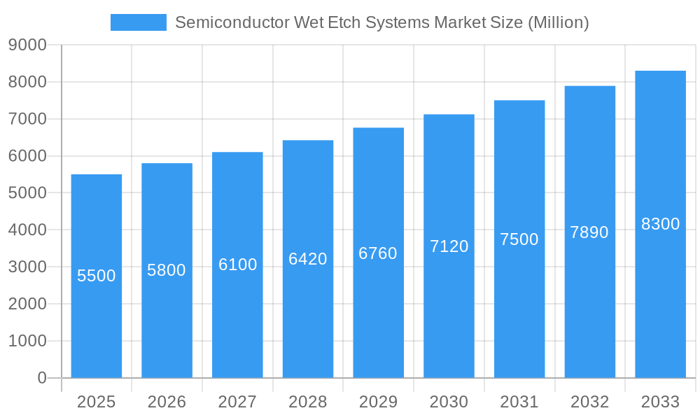
The global Semiconductor Wet Etch Systems Market is poised for substantial expansion, projected to reach a significant valuation by 2033. Driven by the insatiable demand for advanced semiconductors across various sectors like consumer electronics, automotive, and telecommunications, the market is expected to grow at a Compound Annual Growth Rate (CAGR) of 5.35%. This growth is underpinned by the critical role of wet etching processes in fabricating complex integrated circuits. The market's current size, estimated at $5.5 billion in the base year of 2025, will see considerable uplift as technological advancements in chip design and manufacturing continue to accelerate. Key drivers include the increasing complexity of semiconductor architectures, the need for cost-effective etching solutions, and the ongoing miniaturization trend in electronic components. The evolution of smart devices, 5G infrastructure, and the burgeoning Internet of Things (IoT) ecosystem are directly fueling the need for more sophisticated and efficient wet etch systems.
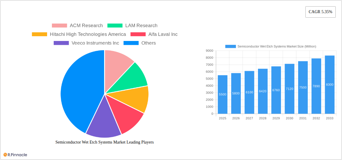
Semiconductor Wet Etch Systems Market Market Size (In Billion)
The market is segmented by type into Isotropic Wet Etching and Anisotropic Wet Etching, catering to diverse fabrication needs, with applications spanning Logic and Memory, Power Devices, MEMS, and Other Applications. The dominance of Logic and Memory segments is anticipated to persist due to the constant innovation and demand for higher performance in these areas. While the market exhibits robust growth, it is not without its challenges. Stringent environmental regulations concerning chemical usage and waste disposal in wet etching processes could pose a restraint. Furthermore, the increasing adoption of dry etching techniques for specific advanced applications might present a competitive pressure. However, the inherent advantages of wet etching, such as its cost-effectiveness for certain processes and its ability to achieve high throughput, ensure its continued relevance and market penetration. Leading companies in this space, including ACM Research and LAM Research, are at the forefront of innovation, developing advanced systems that address these market dynamics and further solidify the market's upward trajectory. Asia, with its established and expanding semiconductor manufacturing base, is expected to lead regional growth, supported by strong investments in advanced fabrication technologies.
Semiconductor Wet Etch Systems Market Company Market Share
Gain unparalleled insights into the dynamic Semiconductor Wet Etch Systems Market with this comprehensive report. Covering the study period from 2019 to 2033, with a base year of 2025, this analysis provides critical market intelligence for industry professionals, including manufacturers, suppliers, investors, and R&D specialists. Uncover detailed segmentation, growth drivers, challenges, and emerging opportunities shaping the future of wet etching technology in semiconductor manufacturing. The market is poised for significant expansion, driven by the relentless demand for advanced logic and memory chips, the burgeoning power device sector, and the miniaturization capabilities offered by MEMS.
Semiconductor Wet Etch Systems Market Market Structure & Innovation Trends
The Semiconductor Wet Etch Systems Market exhibits a moderately concentrated structure, with a few key players dominating market share. Innovation is a primary driver, fueled by the continuous need for higher precision, improved throughput, and reduced environmental impact in semiconductor fabrication. Regulatory frameworks, particularly concerning chemical usage and waste disposal, are increasingly influencing system design and adoption. Product substitutes, such as dry etching techniques, present ongoing competition, necessitating advancements in wet etch efficiency and selectivity. End-user demographics are primarily driven by major semiconductor manufacturers and foundries focused on advanced node production. Mergers and acquisitions (M&A) activity remains a strategic tool for market consolidation and technology acquisition, with deal values often reaching into the hundreds of millions. For instance, the estimated market share of the top 5 players currently stands at approximately 65%, with ongoing consolidation expected to further refine this landscape.
Semiconductor Wet Etch Systems Market Market Dynamics & Trends
The global Semiconductor Wet Etch Systems Market is experiencing robust growth, projected to expand at a Compound Annual Growth Rate (CAGR) of approximately 7.2% from 2025 to 2033. This expansion is propelled by several interconnected market dynamics. The escalating demand for high-performance computing, artificial intelligence, and the Internet of Things (IoT) devices necessitates the production of increasingly complex and miniaturized semiconductor chips. Wet etching, a cost-effective and highly selective process, remains indispensable for critical fabrication steps, particularly in achieving precise feature definitions and wafer cleaning. Technological advancements are continuously enhancing the capabilities of wet etch systems, focusing on improved uniformity, reduced chemical consumption, and greater process control. For example, the introduction of advanced chemistries and automation features is significantly boosting wafer throughput and yield. Consumer preferences, indirectly influencing the semiconductor industry, lean towards smaller, more powerful, and energy-efficient electronic devices, thereby driving innovation in chip design and fabrication processes that rely on sophisticated wet etching. Competitive dynamics are characterized by intense R&D efforts, strategic partnerships, and a focus on delivering solutions that address specific application needs, such as advanced packaging and next-generation memory technologies. Market penetration of advanced wet etch systems is projected to reach over 85% by the end of the forecast period, underscoring their critical role in modern semiconductor manufacturing. The increasing complexity of wafer geometries and the drive towards higher integration density are creating a sustained demand for precise and efficient wet etching solutions. Furthermore, the growing adoption of semiconductor manufacturing in emerging economies is expanding the overall market footprint.
Dominant Regions & Segments in Semiconductor Wet Etch Systems Market
The Asia-Pacific region is currently the dominant force in the Semiconductor Wet Etch Systems Market, largely driven by the significant concentration of semiconductor manufacturing facilities in countries like Taiwan, South Korea, and China. This dominance is supported by robust government initiatives promoting domestic semiconductor production, substantial investments in advanced fabrication technologies, and the presence of leading foundries and integrated device manufacturers (IDMs). Economic policies favoring technology development and expansion of manufacturing infrastructure are key enablers.
Type Segmentation:
- Isotropic Wet Etching: This segment remains crucial for bulk material removal and cleaning applications. Its prevalence is linked to its cost-effectiveness and broad applicability across various semiconductor layers.
- Anisotropic Wet Etching: Driven by the demand for precise feature definition, especially in advanced logic and memory devices, this segment is experiencing significant growth. Innovations in mask technology and etching chemistries are enhancing its capabilities.
Application Segmentation:
- Logic and Memory: This is the largest and fastest-growing application segment, propelled by the relentless demand for higher performance and greater storage capacity in consumer electronics, data centers, and AI applications. The need for sub-10nm lithography and advanced packaging solutions directly fuels demand for sophisticated wet etch systems.
- Power Device: The burgeoning electric vehicle (EV) market and the increasing adoption of renewable energy solutions are driving substantial growth in the power device sector. Wet etching plays a vital role in the fabrication of these devices, contributing to efficiency and reliability.
- MEMS (Micro-Electro-Mechanical Systems): The miniaturization trend across various industries, from automotive to medical devices, is boosting the MEMS market. Wet etching is instrumental in creating the intricate microstructures characteristic of MEMS devices.
- Other Applications: This segment encompasses niche applications in sensors, photonics, and specialized semiconductor devices, contributing steadily to market growth.
The strong presence of leading semiconductor manufacturers in the Asia-Pacific, coupled with continuous technological advancements in etching processes, solidifies its leadership position. Investment in new fab constructions and capacity expansions further reinforces this regional dominance.
Semiconductor Wet Etch Systems Market Product Innovations
Product innovations in the Semiconductor Wet Etch Systems Market are focused on enhancing precision, throughput, and sustainability. Companies are developing advanced single-wafer wet etch systems that offer superior uniformity and reduced chemical waste, crucial for sub-10nm semiconductor manufacturing. Innovations in multi-functional tools, capable of performing both etching and cleaning in a single chamber, are improving process efficiency and reducing manufacturing footprint. The competitive advantage lies in delivering solutions that enable higher yields, lower cost of ownership, and greater process control for advanced logic, memory, and power device applications.
Report Scope & Segmentation Analysis
This report meticulously analyzes the Semiconductor Wet Etch Systems Market across key segmentations to provide a granular understanding of market dynamics. The Type segmentation includes Isotropic Wet Etching and Anisotropic Wet Etching. Isotropic wet etching is characterized by its widespread use in bulk material removal and its cost-effectiveness, catering to a broad range of applications. Anisotropic wet etching, while more complex, is critical for achieving high-resolution patterns and is essential for advanced semiconductor nodes. The Application segmentation comprises Logic and Memory, Power Device, MEMS, and Other Applications. The Logic and Memory segment is driven by the ever-increasing demand for computational power and data storage. The Power Device segment is experiencing rapid expansion due to the growth of electric vehicles and renewable energy. MEMS applications are fueled by miniaturization trends in various consumer and industrial sectors. Each segment is analyzed for its projected market size, growth rates, and competitive landscape.
Key Drivers of Semiconductor Wet Etch Systems Market Growth
The growth of the Semiconductor Wet Etch Systems Market is primarily propelled by the accelerating demand for advanced semiconductors across various industries. Key drivers include:
- Technological Advancements in Chip Manufacturing: The continuous drive for smaller feature sizes, higher transistor densities, and complex 3D architectures in logic and memory devices necessitates precision wet etching capabilities.
- Growth in Emerging Applications: The proliferation of 5G, AI, IoT, and electric vehicles is fueling demand for specialized semiconductors, including power devices and advanced sensors, which rely heavily on wet etching processes.
- Cost-Effectiveness and Selectivity: Wet etching offers a cost-effective and highly selective method for material removal and surface preparation, making it indispensable for many critical fabrication steps.
- Government Initiatives and Investments: Supportive government policies and substantial investments in semiconductor manufacturing infrastructure, particularly in Asia-Pacific, are creating a favorable market environment.
Challenges in the Semiconductor Wet Etch Systems Market Sector
Despite strong growth prospects, the Semiconductor Wet Etch Systems Market faces several challenges that could impact its trajectory. These include:
- Environmental Regulations: Stringent environmental regulations concerning the use and disposal of hazardous chemicals employed in wet etching can lead to increased operational costs and necessitate investment in waste treatment technologies.
- Supply Chain Disruptions: Global supply chain vulnerabilities, including the availability of specialty chemicals and critical components, can affect production timelines and increase lead times for etch systems.
- Intensifying Competition: The market faces competition from alternative technologies, such as dry etching, which may offer advantages in specific applications. This necessitates continuous innovation to maintain market share.
- High Capital Investment: The acquisition and implementation of advanced wet etch systems represent a significant capital investment for semiconductor manufacturers, potentially limiting adoption for smaller players.
Emerging Opportunities in Semiconductor Wet Etch Systems Market
The Semiconductor Wet Etch Systems Market is ripe with emerging opportunities driven by evolving technological landscapes and market demands.
- Advanced Packaging Technologies: The increasing adoption of advanced packaging solutions like fan-out panel-level packaging (FOPLP) presents a significant opportunity for specialized bevel etching and cleaning tools.
- Next-Generation Materials: The exploration and adoption of new semiconductor materials, such as wide-bandgap semiconductors for power electronics, will create demand for tailored wet etching processes.
- Sustainable Etching Solutions: Growing environmental consciousness and regulatory pressure are driving opportunities for vendors developing eco-friendly etching chemistries and highly efficient waste reduction systems.
- Emerging Geographies: The expansion of semiconductor manufacturing capabilities in new regions presents untapped market potential for wet etch system suppliers.
Leading Players in the Semiconductor Wet Etch Systems Market Market
- ACM Research
- LAM Research
- Hitachi High Technologies America
- Alfa Laval Inc
- Veeco Instruments Inc
- JST Manufacturing Inc
- Modutek Corporation
- Inseto
- Shenzhen Dragon Etching Co Ltd
- Micronit BV
Key Developments in Semiconductor Wet Etch Systems Market Industry
- September 2024: ACM Research Inc. unveiled its Ultra C bev-p panel bevel etching tool, tailored for fan-out panel-level packaging (FOPLP) applications. This innovative tool specializes in bevel etching and cleaning for copper-related processes. Notably, it can manage bevel etching on both the front and back sides of the panel, all within a single system. Such versatility boosts process efficiency and bolsters product reliability.
- August 2024: Veeco Instruments Inc. revealed that IBM had chosen its WaferStorm Wet Processing System for Advanced Packaging applications. Furthermore, the two companies have inked a joint development agreement. This collaboration aims to delve into advanced packaging applications, leveraging various wet processing technologies from Veeco. As part of this partnership, the WaferStorm Wet Processing System will find its home at the Albany NanoTech Complex in Albany, NY. This facility is a hub for IBM and its ecosystem partners, who are at the forefront of R&D in advanced packaging and chiplet technologies.
Future Outlook for Semiconductor Wet Etch Systems Market Market
The future outlook for the Semiconductor Wet Etch Systems Market remains highly promising, fueled by the indispensable role of wet etching in advanced semiconductor manufacturing. The accelerating pace of innovation in logic and memory, the rapid expansion of the power device sector driven by electrification, and the continuous miniaturization of MEMS devices will ensure sustained demand for sophisticated wet etch solutions. Strategic collaborations between equipment manufacturers and semiconductor giants, such as the one between Veeco Instruments and IBM, will continue to drive the development of next-generation wet processing technologies for advanced packaging and chiplet integration. The market is expected to witness further technological advancements in areas like single-wafer processing, chemical recycling, and advanced automation, all aimed at improving efficiency, reducing costs, and enhancing environmental sustainability. The growing global semiconductor capacity expansion initiatives will further solidify the market's upward trajectory, making it a crucial component of the future electronics ecosystem.
Semiconductor Wet Etch Systems Market Segmentation
-
1. Type
- 1.1. Isotropic Wet Etching
- 1.2. Anisotropic Wet Etching
-
2. Application
- 2.1. Logic and Memory
- 2.2. Power Device
- 2.3. MEMS
- 2.4. Other Applications
Semiconductor Wet Etch Systems Market Segmentation By Geography
- 1. North America
- 2. Europe
- 3. Asia
- 4. Australia and New Zealand
- 5. Latin America
- 6. Middle East and Africa
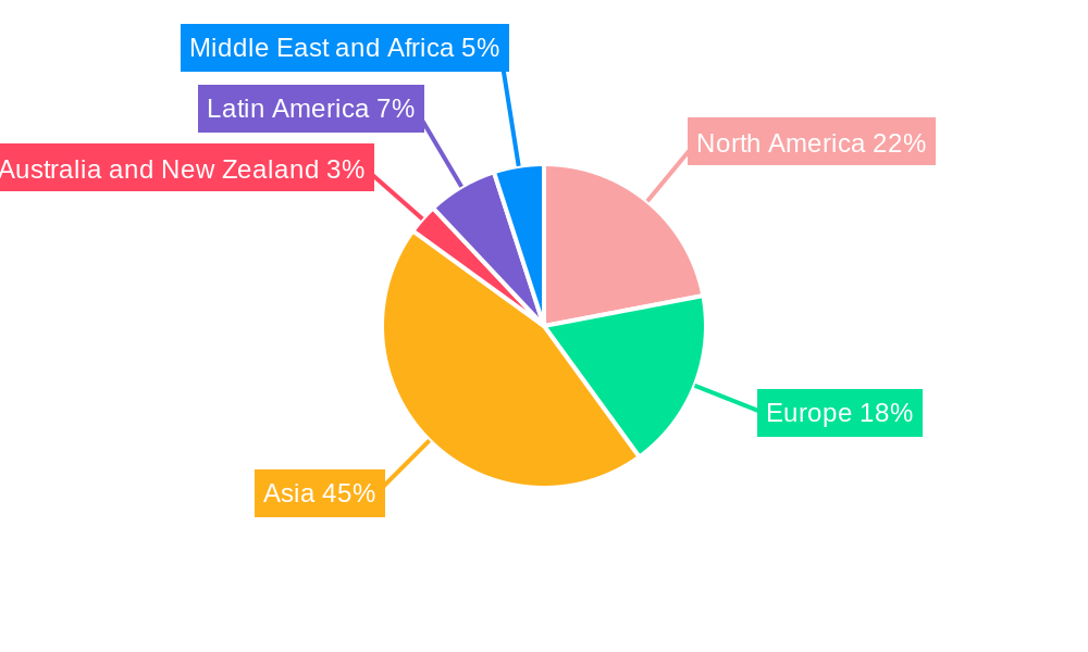
Semiconductor Wet Etch Systems Market Regional Market Share
Geographic Coverage of Semiconductor Wet Etch Systems Market
Semiconductor Wet Etch Systems Market REPORT HIGHLIGHTS
| Aspects | Details |
|---|---|
| Study Period | 2020-2034 |
| Base Year | 2025 |
| Estimated Year | 2026 |
| Forecast Period | 2026-2034 |
| Historical Period | 2020-2025 |
| Growth Rate | CAGR of 5.35% from 2020-2034 |
| Segmentation |
|
Table of Contents
- 1. Introduction
- 1.1. Research Scope
- 1.2. Market Segmentation
- 1.3. Research Objective
- 1.4. Definitions and Assumptions
- 2. Executive Summary
- 2.1. Market Snapshot
- 3. Market Dynamics
- 3.1. Market Drivers
- 3.2. Market Restrains
- 3.3. Market Trends
- 3.4. Market Opportunities
- 4. Market Factor Analysis
- 4.1. Porters Five Forces
- 4.1.1. Bargaining Power of Suppliers
- 4.1.2. Bargaining Power of Buyers
- 4.1.3. Threat of New Entrants
- 4.1.4. Threat of Substitutes
- 4.1.5. Competitive Rivalry
- 4.2. PESTEL analysis
- 4.3. BCG Analysis
- 4.3.1. Stars (High Growth, High Market Share)
- 4.3.2. Cash Cows (Low Growth, High Market Share)
- 4.3.3. Question Mark (High Growth, Low Market Share)
- 4.3.4. Dogs (Low Growth, Low Market Share)
- 4.4. Ansoff Matrix Analysis
- 4.5. Supply Chain Analysis
- 4.6. Regulatory Landscape
- 4.7. Current Market Potential and Opportunity Assessment (TAM–SAM–SOM Framework)
- 4.8. PRI Analyst Note
- 4.1. Porters Five Forces
- 5. Market Analysis, Insights and Forecast 2021-2033
- 5.1. Market Analysis, Insights and Forecast - by Type
- 5.1.1. Isotropic Wet Etching
- 5.1.2. Anisotropic Wet Etching
- 5.2. Market Analysis, Insights and Forecast - by Application
- 5.2.1. Logic and Memory
- 5.2.2. Power Device
- 5.2.3. MEMS
- 5.2.4. Other Applications
- 5.3. Market Analysis, Insights and Forecast - by Region
- 5.3.1. North America
- 5.3.2. Europe
- 5.3.3. Asia
- 5.3.4. Australia and New Zealand
- 5.3.5. Latin America
- 5.3.6. Middle East and Africa
- 5.1. Market Analysis, Insights and Forecast - by Type
- 6. Global Semiconductor Wet Etch Systems Market Analysis, Insights and Forecast, 2021-2033
- 6.1. Market Analysis, Insights and Forecast - by Type
- 6.1.1. Isotropic Wet Etching
- 6.1.2. Anisotropic Wet Etching
- 6.2. Market Analysis, Insights and Forecast - by Application
- 6.2.1. Logic and Memory
- 6.2.2. Power Device
- 6.2.3. MEMS
- 6.2.4. Other Applications
- 6.1. Market Analysis, Insights and Forecast - by Type
- 7. North America Semiconductor Wet Etch Systems Market Analysis, Insights and Forecast, 2020-2032
- 7.1. Market Analysis, Insights and Forecast - by Type
- 7.1.1. Isotropic Wet Etching
- 7.1.2. Anisotropic Wet Etching
- 7.2. Market Analysis, Insights and Forecast - by Application
- 7.2.1. Logic and Memory
- 7.2.2. Power Device
- 7.2.3. MEMS
- 7.2.4. Other Applications
- 7.1. Market Analysis, Insights and Forecast - by Type
- 8. Europe Semiconductor Wet Etch Systems Market Analysis, Insights and Forecast, 2020-2032
- 8.1. Market Analysis, Insights and Forecast - by Type
- 8.1.1. Isotropic Wet Etching
- 8.1.2. Anisotropic Wet Etching
- 8.2. Market Analysis, Insights and Forecast - by Application
- 8.2.1. Logic and Memory
- 8.2.2. Power Device
- 8.2.3. MEMS
- 8.2.4. Other Applications
- 8.1. Market Analysis, Insights and Forecast - by Type
- 9. Asia Semiconductor Wet Etch Systems Market Analysis, Insights and Forecast, 2020-2032
- 9.1. Market Analysis, Insights and Forecast - by Type
- 9.1.1. Isotropic Wet Etching
- 9.1.2. Anisotropic Wet Etching
- 9.2. Market Analysis, Insights and Forecast - by Application
- 9.2.1. Logic and Memory
- 9.2.2. Power Device
- 9.2.3. MEMS
- 9.2.4. Other Applications
- 9.1. Market Analysis, Insights and Forecast - by Type
- 10. Australia and New Zealand Semiconductor Wet Etch Systems Market Analysis, Insights and Forecast, 2020-2032
- 10.1. Market Analysis, Insights and Forecast - by Type
- 10.1.1. Isotropic Wet Etching
- 10.1.2. Anisotropic Wet Etching
- 10.2. Market Analysis, Insights and Forecast - by Application
- 10.2.1. Logic and Memory
- 10.2.2. Power Device
- 10.2.3. MEMS
- 10.2.4. Other Applications
- 10.1. Market Analysis, Insights and Forecast - by Type
- 11. Latin America Semiconductor Wet Etch Systems Market Analysis, Insights and Forecast, 2020-2032
- 11.1. Market Analysis, Insights and Forecast - by Type
- 11.1.1. Isotropic Wet Etching
- 11.1.2. Anisotropic Wet Etching
- 11.2. Market Analysis, Insights and Forecast - by Application
- 11.2.1. Logic and Memory
- 11.2.2. Power Device
- 11.2.3. MEMS
- 11.2.4. Other Applications
- 11.1. Market Analysis, Insights and Forecast - by Type
- 12. Middle East and Africa Semiconductor Wet Etch Systems Market Analysis, Insights and Forecast, 2020-2032
- 12.1. Market Analysis, Insights and Forecast - by Type
- 12.1.1. Isotropic Wet Etching
- 12.1.2. Anisotropic Wet Etching
- 12.2. Market Analysis, Insights and Forecast - by Application
- 12.2.1. Logic and Memory
- 12.2.2. Power Device
- 12.2.3. MEMS
- 12.2.4. Other Applications
- 12.1. Market Analysis, Insights and Forecast - by Type
- 13. Competitive Analysis
- 13.1. Company Profiles
- 13.1.1 ACM Research
- 13.1.1.1. Company Overview
- 13.1.1.2. Products
- 13.1.1.3. Company Financials
- 13.1.1.4. SWOT Analysis
- 13.1.2 LAM Research
- 13.1.2.1. Company Overview
- 13.1.2.2. Products
- 13.1.2.3. Company Financials
- 13.1.2.4. SWOT Analysis
- 13.1.3 Hitachi High Technologies America
- 13.1.3.1. Company Overview
- 13.1.3.2. Products
- 13.1.3.3. Company Financials
- 13.1.3.4. SWOT Analysis
- 13.1.4 Alfa Laval Inc
- 13.1.4.1. Company Overview
- 13.1.4.2. Products
- 13.1.4.3. Company Financials
- 13.1.4.4. SWOT Analysis
- 13.1.5 Veeco Instruments Inc
- 13.1.5.1. Company Overview
- 13.1.5.2. Products
- 13.1.5.3. Company Financials
- 13.1.5.4. SWOT Analysis
- 13.1.6 JST Manufacturing Inc
- 13.1.6.1. Company Overview
- 13.1.6.2. Products
- 13.1.6.3. Company Financials
- 13.1.6.4. SWOT Analysis
- 13.1.7 Modutek Corporation
- 13.1.7.1. Company Overview
- 13.1.7.2. Products
- 13.1.7.3. Company Financials
- 13.1.7.4. SWOT Analysis
- 13.1.8 Inseto
- 13.1.8.1. Company Overview
- 13.1.8.2. Products
- 13.1.8.3. Company Financials
- 13.1.8.4. SWOT Analysis
- 13.1.9 Shenzhen Dragon Etching Co Ltd
- 13.1.9.1. Company Overview
- 13.1.9.2. Products
- 13.1.9.3. Company Financials
- 13.1.9.4. SWOT Analysis
- 13.1.10 Micronit BV*List Not Exhaustive
- 13.1.10.1. Company Overview
- 13.1.10.2. Products
- 13.1.10.3. Company Financials
- 13.1.10.4. SWOT Analysis
- 13.1.1 ACM Research
- 13.2. Market Entropy
- 13.2.1 Company's Key Areas Served
- 13.2.2 Recent Developments
- 13.3. Company Market Share Analysis 2025
- 13.3.1 Top 5 Companies Market Share Analysis
- 13.3.2 Top 3 Companies Market Share Analysis
- 13.4. List of Potential Customers
- 14. Research Methodology
List of Figures
- Figure 1: Global Semiconductor Wet Etch Systems Market Revenue Breakdown (Million, %) by Region 2025 & 2033
- Figure 2: Global Semiconductor Wet Etch Systems Market Volume Breakdown (Billion, %) by Region 2025 & 2033
- Figure 3: North America Semiconductor Wet Etch Systems Market Revenue (Million), by Type 2025 & 2033
- Figure 4: North America Semiconductor Wet Etch Systems Market Volume (Billion), by Type 2025 & 2033
- Figure 5: North America Semiconductor Wet Etch Systems Market Revenue Share (%), by Type 2025 & 2033
- Figure 6: North America Semiconductor Wet Etch Systems Market Volume Share (%), by Type 2025 & 2033
- Figure 7: North America Semiconductor Wet Etch Systems Market Revenue (Million), by Application 2025 & 2033
- Figure 8: North America Semiconductor Wet Etch Systems Market Volume (Billion), by Application 2025 & 2033
- Figure 9: North America Semiconductor Wet Etch Systems Market Revenue Share (%), by Application 2025 & 2033
- Figure 10: North America Semiconductor Wet Etch Systems Market Volume Share (%), by Application 2025 & 2033
- Figure 11: North America Semiconductor Wet Etch Systems Market Revenue (Million), by Country 2025 & 2033
- Figure 12: North America Semiconductor Wet Etch Systems Market Volume (Billion), by Country 2025 & 2033
- Figure 13: North America Semiconductor Wet Etch Systems Market Revenue Share (%), by Country 2025 & 2033
- Figure 14: North America Semiconductor Wet Etch Systems Market Volume Share (%), by Country 2025 & 2033
- Figure 15: Europe Semiconductor Wet Etch Systems Market Revenue (Million), by Type 2025 & 2033
- Figure 16: Europe Semiconductor Wet Etch Systems Market Volume (Billion), by Type 2025 & 2033
- Figure 17: Europe Semiconductor Wet Etch Systems Market Revenue Share (%), by Type 2025 & 2033
- Figure 18: Europe Semiconductor Wet Etch Systems Market Volume Share (%), by Type 2025 & 2033
- Figure 19: Europe Semiconductor Wet Etch Systems Market Revenue (Million), by Application 2025 & 2033
- Figure 20: Europe Semiconductor Wet Etch Systems Market Volume (Billion), by Application 2025 & 2033
- Figure 21: Europe Semiconductor Wet Etch Systems Market Revenue Share (%), by Application 2025 & 2033
- Figure 22: Europe Semiconductor Wet Etch Systems Market Volume Share (%), by Application 2025 & 2033
- Figure 23: Europe Semiconductor Wet Etch Systems Market Revenue (Million), by Country 2025 & 2033
- Figure 24: Europe Semiconductor Wet Etch Systems Market Volume (Billion), by Country 2025 & 2033
- Figure 25: Europe Semiconductor Wet Etch Systems Market Revenue Share (%), by Country 2025 & 2033
- Figure 26: Europe Semiconductor Wet Etch Systems Market Volume Share (%), by Country 2025 & 2033
- Figure 27: Asia Semiconductor Wet Etch Systems Market Revenue (Million), by Type 2025 & 2033
- Figure 28: Asia Semiconductor Wet Etch Systems Market Volume (Billion), by Type 2025 & 2033
- Figure 29: Asia Semiconductor Wet Etch Systems Market Revenue Share (%), by Type 2025 & 2033
- Figure 30: Asia Semiconductor Wet Etch Systems Market Volume Share (%), by Type 2025 & 2033
- Figure 31: Asia Semiconductor Wet Etch Systems Market Revenue (Million), by Application 2025 & 2033
- Figure 32: Asia Semiconductor Wet Etch Systems Market Volume (Billion), by Application 2025 & 2033
- Figure 33: Asia Semiconductor Wet Etch Systems Market Revenue Share (%), by Application 2025 & 2033
- Figure 34: Asia Semiconductor Wet Etch Systems Market Volume Share (%), by Application 2025 & 2033
- Figure 35: Asia Semiconductor Wet Etch Systems Market Revenue (Million), by Country 2025 & 2033
- Figure 36: Asia Semiconductor Wet Etch Systems Market Volume (Billion), by Country 2025 & 2033
- Figure 37: Asia Semiconductor Wet Etch Systems Market Revenue Share (%), by Country 2025 & 2033
- Figure 38: Asia Semiconductor Wet Etch Systems Market Volume Share (%), by Country 2025 & 2033
- Figure 39: Australia and New Zealand Semiconductor Wet Etch Systems Market Revenue (Million), by Type 2025 & 2033
- Figure 40: Australia and New Zealand Semiconductor Wet Etch Systems Market Volume (Billion), by Type 2025 & 2033
- Figure 41: Australia and New Zealand Semiconductor Wet Etch Systems Market Revenue Share (%), by Type 2025 & 2033
- Figure 42: Australia and New Zealand Semiconductor Wet Etch Systems Market Volume Share (%), by Type 2025 & 2033
- Figure 43: Australia and New Zealand Semiconductor Wet Etch Systems Market Revenue (Million), by Application 2025 & 2033
- Figure 44: Australia and New Zealand Semiconductor Wet Etch Systems Market Volume (Billion), by Application 2025 & 2033
- Figure 45: Australia and New Zealand Semiconductor Wet Etch Systems Market Revenue Share (%), by Application 2025 & 2033
- Figure 46: Australia and New Zealand Semiconductor Wet Etch Systems Market Volume Share (%), by Application 2025 & 2033
- Figure 47: Australia and New Zealand Semiconductor Wet Etch Systems Market Revenue (Million), by Country 2025 & 2033
- Figure 48: Australia and New Zealand Semiconductor Wet Etch Systems Market Volume (Billion), by Country 2025 & 2033
- Figure 49: Australia and New Zealand Semiconductor Wet Etch Systems Market Revenue Share (%), by Country 2025 & 2033
- Figure 50: Australia and New Zealand Semiconductor Wet Etch Systems Market Volume Share (%), by Country 2025 & 2033
- Figure 51: Latin America Semiconductor Wet Etch Systems Market Revenue (Million), by Type 2025 & 2033
- Figure 52: Latin America Semiconductor Wet Etch Systems Market Volume (Billion), by Type 2025 & 2033
- Figure 53: Latin America Semiconductor Wet Etch Systems Market Revenue Share (%), by Type 2025 & 2033
- Figure 54: Latin America Semiconductor Wet Etch Systems Market Volume Share (%), by Type 2025 & 2033
- Figure 55: Latin America Semiconductor Wet Etch Systems Market Revenue (Million), by Application 2025 & 2033
- Figure 56: Latin America Semiconductor Wet Etch Systems Market Volume (Billion), by Application 2025 & 2033
- Figure 57: Latin America Semiconductor Wet Etch Systems Market Revenue Share (%), by Application 2025 & 2033
- Figure 58: Latin America Semiconductor Wet Etch Systems Market Volume Share (%), by Application 2025 & 2033
- Figure 59: Latin America Semiconductor Wet Etch Systems Market Revenue (Million), by Country 2025 & 2033
- Figure 60: Latin America Semiconductor Wet Etch Systems Market Volume (Billion), by Country 2025 & 2033
- Figure 61: Latin America Semiconductor Wet Etch Systems Market Revenue Share (%), by Country 2025 & 2033
- Figure 62: Latin America Semiconductor Wet Etch Systems Market Volume Share (%), by Country 2025 & 2033
- Figure 63: Middle East and Africa Semiconductor Wet Etch Systems Market Revenue (Million), by Type 2025 & 2033
- Figure 64: Middle East and Africa Semiconductor Wet Etch Systems Market Volume (Billion), by Type 2025 & 2033
- Figure 65: Middle East and Africa Semiconductor Wet Etch Systems Market Revenue Share (%), by Type 2025 & 2033
- Figure 66: Middle East and Africa Semiconductor Wet Etch Systems Market Volume Share (%), by Type 2025 & 2033
- Figure 67: Middle East and Africa Semiconductor Wet Etch Systems Market Revenue (Million), by Application 2025 & 2033
- Figure 68: Middle East and Africa Semiconductor Wet Etch Systems Market Volume (Billion), by Application 2025 & 2033
- Figure 69: Middle East and Africa Semiconductor Wet Etch Systems Market Revenue Share (%), by Application 2025 & 2033
- Figure 70: Middle East and Africa Semiconductor Wet Etch Systems Market Volume Share (%), by Application 2025 & 2033
- Figure 71: Middle East and Africa Semiconductor Wet Etch Systems Market Revenue (Million), by Country 2025 & 2033
- Figure 72: Middle East and Africa Semiconductor Wet Etch Systems Market Volume (Billion), by Country 2025 & 2033
- Figure 73: Middle East and Africa Semiconductor Wet Etch Systems Market Revenue Share (%), by Country 2025 & 2033
- Figure 74: Middle East and Africa Semiconductor Wet Etch Systems Market Volume Share (%), by Country 2025 & 2033
List of Tables
- Table 1: Global Semiconductor Wet Etch Systems Market Revenue Million Forecast, by Type 2020 & 2033
- Table 2: Global Semiconductor Wet Etch Systems Market Volume Billion Forecast, by Type 2020 & 2033
- Table 3: Global Semiconductor Wet Etch Systems Market Revenue Million Forecast, by Application 2020 & 2033
- Table 4: Global Semiconductor Wet Etch Systems Market Volume Billion Forecast, by Application 2020 & 2033
- Table 5: Global Semiconductor Wet Etch Systems Market Revenue Million Forecast, by Region 2020 & 2033
- Table 6: Global Semiconductor Wet Etch Systems Market Volume Billion Forecast, by Region 2020 & 2033
- Table 7: Global Semiconductor Wet Etch Systems Market Revenue Million Forecast, by Type 2020 & 2033
- Table 8: Global Semiconductor Wet Etch Systems Market Volume Billion Forecast, by Type 2020 & 2033
- Table 9: Global Semiconductor Wet Etch Systems Market Revenue Million Forecast, by Application 2020 & 2033
- Table 10: Global Semiconductor Wet Etch Systems Market Volume Billion Forecast, by Application 2020 & 2033
- Table 11: Global Semiconductor Wet Etch Systems Market Revenue Million Forecast, by Country 2020 & 2033
- Table 12: Global Semiconductor Wet Etch Systems Market Volume Billion Forecast, by Country 2020 & 2033
- Table 13: Global Semiconductor Wet Etch Systems Market Revenue Million Forecast, by Type 2020 & 2033
- Table 14: Global Semiconductor Wet Etch Systems Market Volume Billion Forecast, by Type 2020 & 2033
- Table 15: Global Semiconductor Wet Etch Systems Market Revenue Million Forecast, by Application 2020 & 2033
- Table 16: Global Semiconductor Wet Etch Systems Market Volume Billion Forecast, by Application 2020 & 2033
- Table 17: Global Semiconductor Wet Etch Systems Market Revenue Million Forecast, by Country 2020 & 2033
- Table 18: Global Semiconductor Wet Etch Systems Market Volume Billion Forecast, by Country 2020 & 2033
- Table 19: Global Semiconductor Wet Etch Systems Market Revenue Million Forecast, by Type 2020 & 2033
- Table 20: Global Semiconductor Wet Etch Systems Market Volume Billion Forecast, by Type 2020 & 2033
- Table 21: Global Semiconductor Wet Etch Systems Market Revenue Million Forecast, by Application 2020 & 2033
- Table 22: Global Semiconductor Wet Etch Systems Market Volume Billion Forecast, by Application 2020 & 2033
- Table 23: Global Semiconductor Wet Etch Systems Market Revenue Million Forecast, by Country 2020 & 2033
- Table 24: Global Semiconductor Wet Etch Systems Market Volume Billion Forecast, by Country 2020 & 2033
- Table 25: Global Semiconductor Wet Etch Systems Market Revenue Million Forecast, by Type 2020 & 2033
- Table 26: Global Semiconductor Wet Etch Systems Market Volume Billion Forecast, by Type 2020 & 2033
- Table 27: Global Semiconductor Wet Etch Systems Market Revenue Million Forecast, by Application 2020 & 2033
- Table 28: Global Semiconductor Wet Etch Systems Market Volume Billion Forecast, by Application 2020 & 2033
- Table 29: Global Semiconductor Wet Etch Systems Market Revenue Million Forecast, by Country 2020 & 2033
- Table 30: Global Semiconductor Wet Etch Systems Market Volume Billion Forecast, by Country 2020 & 2033
- Table 31: Global Semiconductor Wet Etch Systems Market Revenue Million Forecast, by Type 2020 & 2033
- Table 32: Global Semiconductor Wet Etch Systems Market Volume Billion Forecast, by Type 2020 & 2033
- Table 33: Global Semiconductor Wet Etch Systems Market Revenue Million Forecast, by Application 2020 & 2033
- Table 34: Global Semiconductor Wet Etch Systems Market Volume Billion Forecast, by Application 2020 & 2033
- Table 35: Global Semiconductor Wet Etch Systems Market Revenue Million Forecast, by Country 2020 & 2033
- Table 36: Global Semiconductor Wet Etch Systems Market Volume Billion Forecast, by Country 2020 & 2033
- Table 37: Global Semiconductor Wet Etch Systems Market Revenue Million Forecast, by Type 2020 & 2033
- Table 38: Global Semiconductor Wet Etch Systems Market Volume Billion Forecast, by Type 2020 & 2033
- Table 39: Global Semiconductor Wet Etch Systems Market Revenue Million Forecast, by Application 2020 & 2033
- Table 40: Global Semiconductor Wet Etch Systems Market Volume Billion Forecast, by Application 2020 & 2033
- Table 41: Global Semiconductor Wet Etch Systems Market Revenue Million Forecast, by Country 2020 & 2033
- Table 42: Global Semiconductor Wet Etch Systems Market Volume Billion Forecast, by Country 2020 & 2033
Frequently Asked Questions
1. What is the projected Compound Annual Growth Rate (CAGR) of the Semiconductor Wet Etch Systems Market?
The projected CAGR is approximately 5.35%.
2. Which companies are prominent players in the Semiconductor Wet Etch Systems Market?
Key companies in the market include ACM Research, LAM Research, Hitachi High Technologies America, Alfa Laval Inc, Veeco Instruments Inc, JST Manufacturing Inc, Modutek Corporation, Inseto, Shenzhen Dragon Etching Co Ltd, Micronit BV*List Not Exhaustive.
3. What are the main segments of the Semiconductor Wet Etch Systems Market?
The market segments include Type, Application.
4. Can you provide details about the market size?
The market size is estimated to be USD 5.5 Million as of 2022.
5. What are some drivers contributing to market growth?
Increasing Application in Consumer Electronic Devices. Automotive. and Aerospace; Proliferation of Artificial Intelligence. IoT. and Connected Devices across Industry Verticals.
6. What are the notable trends driving market growth?
The MEMS Segment is Expected to Observe Significant Growth.
7. Are there any restraints impacting market growth?
Increasing Application in Consumer Electronic Devices. Automotive. and Aerospace; Proliferation of Artificial Intelligence. IoT. and Connected Devices across Industry Verticals.
8. Can you provide examples of recent developments in the market?
September 2024: ACM Research Inc. unveiled its Ultra C bev-p panel bevel etching tool, tailored for fan-out panel-level packaging (FOPLP) applications. This innovative tool specializes in bevel etching and cleaning for copper-related processes. Notably, it can manage bevel etching on both the front and back sides of the panel, all within a single system. Such versatility boosts process efficiency and bolsters product reliability.August 2024: Veeco Instruments Inc. revealed that IBM had chosen its WaferStorm Wet Processing System for Advanced Packaging applications. Furthermore, the two companies have inked a joint development agreement. This collaboration aims to delve into advanced packaging applications, leveraging various wet processing technologies from Veeco. As part of this partnership, the WaferStorm Wet Processing System will find its home at the Albany NanoTech Complex in Albany, NY. This facility is a hub for IBM and its ecosystem partners, who are at the forefront of R&D in advanced packaging and chiplet technologies.
9. What pricing options are available for accessing the report?
Pricing options include single-user, multi-user, and enterprise licenses priced at USD 4750, USD 5250, and USD 8750 respectively.
10. Is the market size provided in terms of value or volume?
The market size is provided in terms of value, measured in Million and volume, measured in Billion.
11. Are there any specific market keywords associated with the report?
Yes, the market keyword associated with the report is "Semiconductor Wet Etch Systems Market," which aids in identifying and referencing the specific market segment covered.
12. How do I determine which pricing option suits my needs best?
The pricing options vary based on user requirements and access needs. Individual users may opt for single-user licenses, while businesses requiring broader access may choose multi-user or enterprise licenses for cost-effective access to the report.
13. Are there any additional resources or data provided in the Semiconductor Wet Etch Systems Market report?
While the report offers comprehensive insights, it's advisable to review the specific contents or supplementary materials provided to ascertain if additional resources or data are available.
14. How can I stay updated on further developments or reports in the Semiconductor Wet Etch Systems Market?
To stay informed about further developments, trends, and reports in the Semiconductor Wet Etch Systems Market, consider subscribing to industry newsletters, following relevant companies and organizations, or regularly checking reputable industry news sources and publications.
Methodology
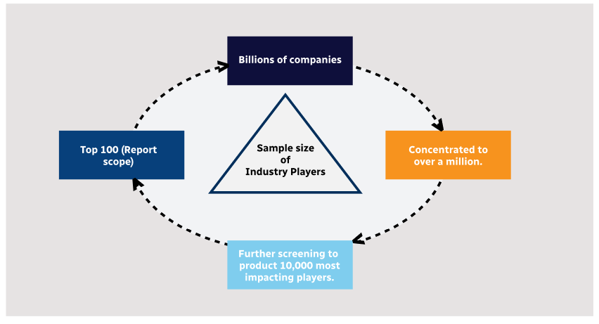
Step 1 - Identification of Relevant Samples Size from Population Database

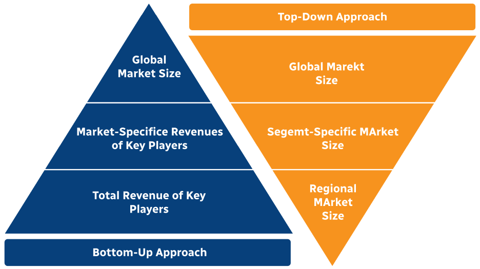
Step 2 - Approaches for Defining Global Market Size (Value, Volume* & Price*)
Note*: In applicable scenarios
Step 3 - Data Sources
Primary Research
- Web Analytics
- Survey Reports
- Research Institute
- Latest Research Reports
- Opinion Leaders
Secondary Research
- Annual Reports
- White Paper
- Latest Press Release
- Industry Association
- Paid Database
- Investor Presentations

Step 4 - Data Triangulation
Involves using different sources of information in order to increase the validity of a study
These sources are likely to be stakeholders in a program - participants, other researchers, program staff, other community members, and so on.
Then we put all data in single framework & apply various statistical tools to find out the dynamic on the market.
During the analysis stage, feedback from the stakeholder groups would be compared to determine areas of agreement as well as areas of divergence